SV4. Differences between ASIC and FPGA RTL Coding
Video Tutorial
Watch this comprehensive video explanation of differences between FPGA and ASIC RTL coding:
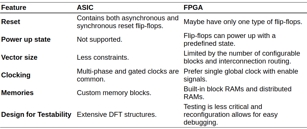
Reset
- ASIC: Standard cell library contains both asynchronous and synchronous reset flip-flops.
- FPGA: Maybe have only one type of flip-flops (Both Xilinx and Altera recommends synchronous reset). Synthesis tools utilize extra logic to map the unsupported flip-flop type.
Power up state
- ASIC: Not supported.
- FPGA: Flip-flops can power up with a predefined state.
Vector size
- ASIC: Less constraints.
- FPGA: Limited by the number of configurable blocks and interconnection routing.
Clocking
- ASIC: Multi-phase and gated clocks are common for reducing power consumption.
- FPGA: Prefer single global clock with enable signals; avoid gated clocks.
Memories
- ASIC: Custom memory blocks. May have different memory structure than FPGA.
- FPGA: Use built-in block RAMs and distributed RAMs.
Design for Testability (DFT)
- ASIC: Extensive DFT structures (Scan Chains, Built-In Self-Test (BIST)).
- FPGA: Minimal DFT, as testing is less critical and reconfiguration allows for easy debugging.
Examples:
Different reset approaches
// ASIC-style with asynchronous reset
module asic_counter (
  input  logic        clk,
  input  logic        rst_n,  // Active low asynchronous reset
  output logic [7:0]  count
);

  always_ff @(posedge clk or negedge rst_n) begin
    if (!rst_n)
      count <= 8'h00;
    else
      count <= count + 1'b1;
  end

endmodule

// FPGA-style with synchronous reset
module fpga_counter (
  input  logic        clk,
  input  logic        rst,    // Active high synchronous reset
  output logic [7:0]  count
);

  always_ff @(posedge clk) begin
    if (rst)
      count <= 8'h00;
    else
      count <= count + 1'b1;
  end

endmodule
Clock Gating Examples
// ASIC-style with clock gating
module asic_clock_gating (
  input  logic clk_in,
  input  logic enable,
  output logic clk_out
);
  logic enable_latch;

  // Latch to prevent glitches on enable signal
  always_latch begin
    if (!clk_in)
      enable_latch <= enable;
  end

  // Gated clock output
  assign clk_out = clk_in & enable_latch;
endmodule

// FPGA-style with clock enable
module fpga_clock_enable (
  input  logic        clk,
  input  logic        enable,
  input  logic        data_in,
  output logic [7:0]  data_out
);

  always_ff @(posedge clk) begin
    if (enable)
      data_out <= data_in;
    // When enable is low, register maintains its value
  end
endmodule