SV2. Comparing FPGA and ASIC Design Processes
This article provides a comparative analysis of the design processes for both FPGA and ASIC.
Video Tutorial
Watch this comprehensive video explanation of differences between FPGA and ASIC design flows:
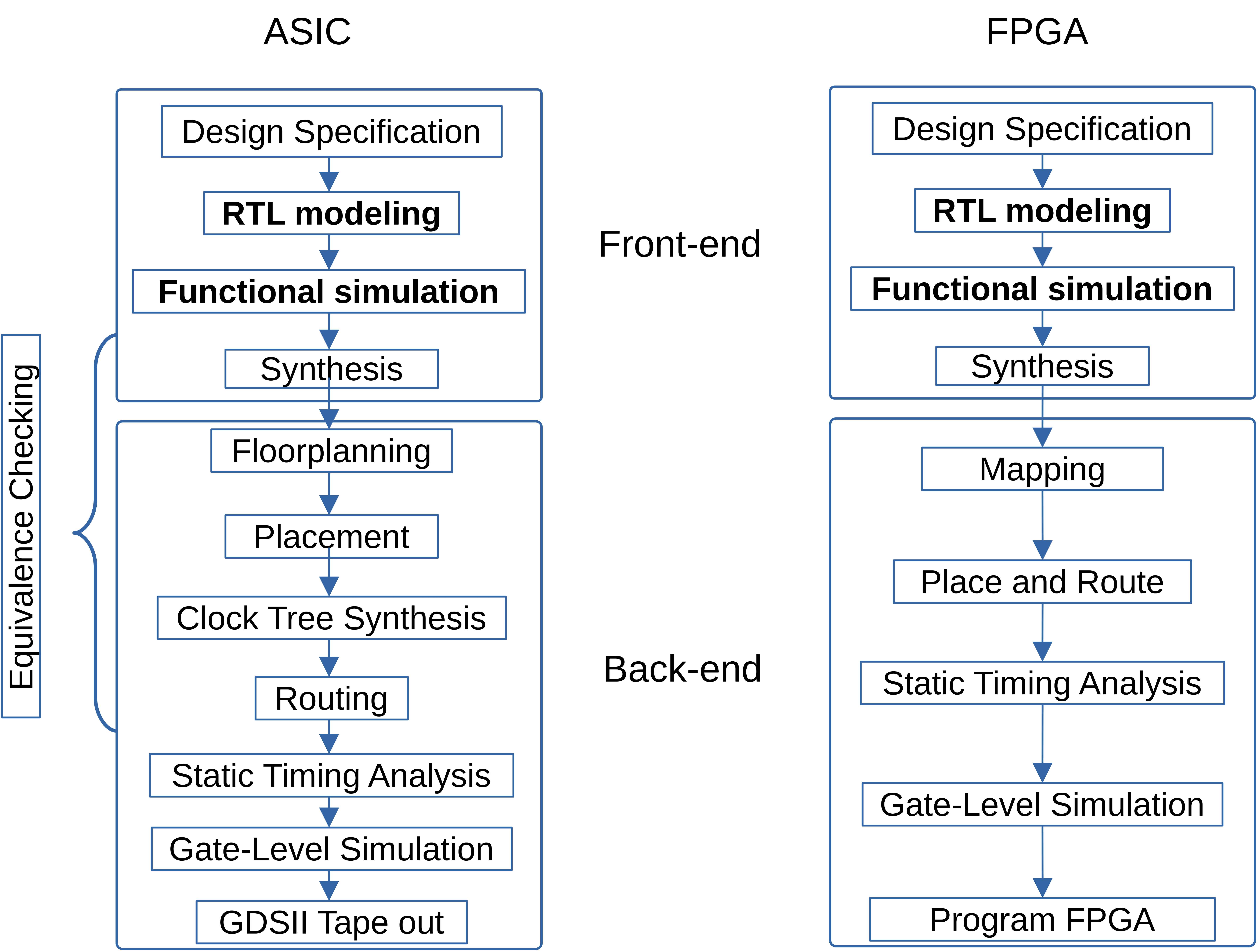
Design Specification
Define the detailed system requirements and specifications with high-level block diagrams in a document, used as a reference for design engineers.
RTL Modeling
Use hardware description languages (HDL) like SystemVerilog to model hardware.
Functional Simulation
Perform simulation to verify that the design behaves as expected based on its functionality without considering delays and timing violations.
Synthesis
Transforms RTL designs into logic gates based on the technology library and user-defined constraints.
Floorplanning (ASIC)
Define the size and shape of the chip, determine optimal locations and sizes of Functional Design Blocks, Macros (memory and analog circuits), I/O pad placement, and plan power distribution.
Mapping (FPGA)
Assign the functions to existing logic blocks, including implementing the combinational logic using look-up tables (LUTs), sequential logics onto flip-flops, and memories into the block RAMs.
Placement (ASIC)
Place the standard cells after Floorplanning.
Placement (FPGA)
Determine the location of logic blocks.
Routing
Connect gates and macros in metal layers.
Clock Tree (ASIC)
Insert clock buffers and inverters in the clock path to optimize clock skew and latency.
Logic Equivalence Check (LEC)
Formal verification technique to determine if two representations of a digital circuit are functionally equivalent.
Formal Verification
A method to check design correctness using mathematical techniques.
Static Timing Analysis (STA)
Check digital circuits for timing without transistor-level simulations, using cell delays from the standard cell library and net delays from parasitic information provided by wire-load models (before physical implementation) and physical libraries after placement and routing.
Gate-Level Sim (GLS)
Simulate the design at the gate (logic) level to verify the functionality of the design after synthesis.
Program (FPGA)
Generate the bitstream that defines the configuration of the logic blocks in FPGA and load the bitstream file to the FPGA.
GDSII (ASIC)
The final step where the design layout is sent to the fabrication house (fab) or foundry for manufacturing. Depending on the technology, chip size, and volume, the cost varies between hundreds of thousands to millions. For 22nm, the cost is in the order of $100,000.
Design Iterations
Verification (functional simulation, GLS, LEC) is highly iterative, with feedback loops to the design stage.