Learn FPGA Development
Most of what you need to learn FPGA design on Xilinx (AMD) devices is free: official courses and workshops, videos, hands-on tutorials, and a large library of user guides and data sheets. The hard part is where to find each document and which document to open first. This post collects them in one place.
Part 1 covers training, videos, and tutorials. Part 2 lists the AMD documents, grouped by topic and device family, and ends with a suggested reading order. Xilinx is now part of AMD, so all former Xilinx material lives on AMD sites today. I checked every link on October 2026.
Table of Contents
- Table of Contents
- Part 1: Training and Videos
- Part 2: Documents
Part 1: Training and Videos
Official AMD Training
AMD Customer Training
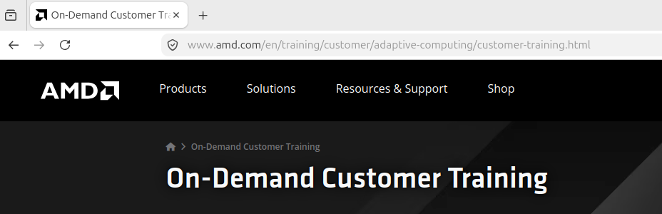
AMD offers official training for Vivado, Vitis, Versal, Zynq, and Kria in two places. The On-Demand Customer Training page lists self-paced courses: a few introductory ones are free, and the full curriculum is paid. The paid courses include the Designing FPGAs Using the Vivado Design Suite series, UltraFast Design Methodology, Design Closure Techniques, and courses on HLS, Versal, and embedded Linux. The Customer Training Center catalog also lists free, live virtual workshops that AMD sponsors and its regional training partners (such as BLT, Doulos, and PLC2) deliver. The topics change during the year, so check the catalog for the current schedule.
- On-Demand Customer Training Self-paced courses. Partly free.
- Free AMD workshops Current free workshops in the Customer Training Center. Free, registration required.
AMD University Program

The AMD University Program (AUP) supports universities with hardware and software donations, access to research clusters (the AMD AI & HPC Cluster and the HACC program), and teaching materials. Membership is for faculty and researchers who enroll with an academic email address. Students do not need to enroll: the public Adaptive and Embedded Computing Training page links to AUP’s lab-based tutorials on GitHub for the Vivado flow, Zynq embedded design, HLS, Vitis, and AI Engines. Most of these labs were written for tool versions from 2021 to 2024, so expect small differences in newer releases.
- AMD University Program Program overview and membership. Free for eligible faculty and researchers.
- Adaptive and Embedded Computing Training Public tutorials and labs. Free.
- Vivado FPGA Design Flow labs AUP’s six-lab Vivado workshop: synthesis, implementation, I/O planning, simulation, static timing analysis, and debug, written for Vivado 2021.2 and the PYNQ-Z2 and Boolean boards. Free.
Free Workshops and Webinars from AMD Training Partners
AMD Authorized Training Providers sell full courses, but they also run free events, many of them sponsored by AMD. AMD’s Authorized Training Providers page lists them by region; the three below run regular free events.
BLT
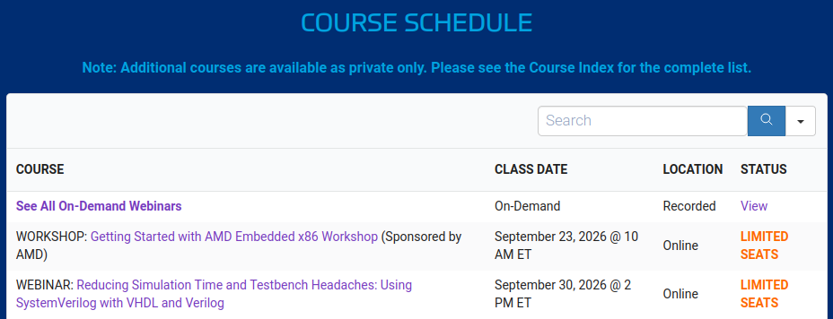
BLT (Bottom Line Technologies) is an AMD Authorized Training Provider in the US. It runs free live webinars, which are recorded and available on demand afterwards, and free workshops on Vivado, timing closure, AXI, and embedded design. On the course calendar, the free workshops are marked “(Sponsored by AMD)”. The regular courses are paid.
- BLT webinar series Free webinars, live and on demand, and free workshops. Free, registration required.
- BLT course calendar All scheduled courses, paid and free.
Doulos

Doulos is a training company for hardware design and verification languages and FPGA design. Its KnowHow workshops are occasional online and in-person events; the ones sponsored by AMD are free to attend (each event page says so). Recent topics have included the AMD Embedded Development Framework, the Vivado AI Assistant, and Versal AI Engines. Doulos also runs free one-hour webinars, many of them available on demand, and publishes free articles and reference guides on VHDL, Verilog, SystemVerilog, and FPGA design.
- Doulos KnowHow Workshops Occasional workshops. Free when sponsored, registration required.
- Doulos webinars Live and on-demand webinars. Free.
- Doulos KnowHow Articles, tutorials, and reference guides. Free.
PLC2
PLC2 (Programmable Logic Competence Centre) is an AMD Authorized Training Provider based in Germany that serves Europe. Besides its paid courses, it runs free one-hour webinars, most of them available on demand (recent topics include FPGA timing constraints and clock domain crossing), and free one-day technical seminars held on site.
- PLC2 webinars One-hour technical webinars, live and on demand. Free.
- PLC2 seminars One-day technical seminars. Free, registration required.
Videos
AMD no longer updates the old Xilinx YouTube channel. The official tool videos are now playlists on the main AMD channel.
- Vivado Design Suite playlist Short official walkthroughs and feature demos for Vivado.
- Vitis Software Developer Tools playlist Short official walkthroughs and feature demos for the Vitis tools.
- More AMD playlists Other adaptive computing playlists on the AMD channel: Vivado for Versal, Vivado for Spartan UltraScale+, AMD Embedded Development Framework, and Vitis Tools for Versal AI Engines.
- Vivado QuickTake: Introduction to Clock Constraints A short AMD video on defining clocks in XDC. Two related QuickTake videos cover Clock Group Constraints and Using the XDC Constraint Editor. Good companions to UG903.
- Nandland on YouTube Russell Merrick’s beginner-friendly videos on core FPGA concepts such as clocks, state machines, and metastability, in both VHDL and Verilog. His website, nandland.com, has matching written tutorials.
The BLT and Doulos webinars listed above are also recorded and available on demand.
Hands-On Tutorials
- Vivado Design Tutorials AMD’s official Vivado tutorials on GitHub, covering general design flows and features specific to UltraScale+ and Versal. Each tutorial states the Vivado release it was tested with.
- Vitis Tutorials AMD’s official step-by-step tutorials for HLS, embedded software, AI Engines, and acceleration. There is one branch per tool release.
- Vitis HLS Introductory Examples Small, self-contained HLS examples, each showing one pragma or interface pattern (pipelining, array partitioning, AXI interfaces, dataflow), with test benches and run scripts. A good companion to UG1399.
- PYNQ An open-source AMD project for controlling Zynq, Zynq UltraScale+, Kria, and Alveo designs from Python and Jupyter notebooks, with documentation, example overlays, and a forum. You need a supported board to run it.
AMD Support Articles
Design and Debug Techniques Blog
AMD support engineers publish worked examples on Vivado, IP, timing, debug, and embedded topics in the Design and Debug Techniques Blog on the Adaptive Support community. One useful index there is Xilinx Video Series and Blog Posts: a set of written tutorials on building and debugging video-processing pipelines with AMD video IP (Test Pattern Generator, AXI4-Stream Video, VDMA, and VPSS), from a beginner series up to advanced designs. Despite the name, these are articles, not recorded videos.

- Design and Debug Techniques Blog Worked examples from AMD support engineers. Free.
- Xilinx Video Series and Blog Posts Index of the video-processing tutorials. Free.
Community Resources
These sites are run by independent engineers and are free to read.
- HDLBits Short Verilog exercises checked by an online simulator, from basic gates to state machines. Good practice without installing any tools.
- ZipCPU Dan Gisselquist’s blog on Verilog design, formal verification with SymbiYosys, and AXI bus design and debugging, plus a free beginner tutorial that uses Verilator.
- MicroZed Chronicles Adam Taylor’s weekly blog on practical AMD FPGA and SoC design (Zynq, Versal, Spartan, Vivado, and Vitis), running for more than ten years.
- FPGA Developer Jeff Johnson’s tutorials and open-source reference designs for AMD boards, covering PCIe, Ethernet, MIPI cameras, and embedded Linux.
Part 2: Documents
AMD publishes a user guide (UG), product guide (PG), data sheet (DS), white paper (WP), or architecture manual (AM) for nearly every tool, IP core, and device. The lists below group the ones worth knowing by topic. Start with How to Find Documents and Start Here. In the device and SoC sections, read only the set for your family.
How to Find Documents
- docs.amd.com AMD’s documentation portal. Search by document number (for example UG949) or by title, and filter by product, document type, and tool version. The links in this post have no version number in them, so they open the latest release. Newer documents open as HTML pages (
/r/en-US/...) and older ones as PDFs (/v/u/en-US/...); if you build a link yourself and get a 404, try the other form. - UG1793 Vivado Design Suite Landing Page. AMD’s index of every Vivado document for the current release.
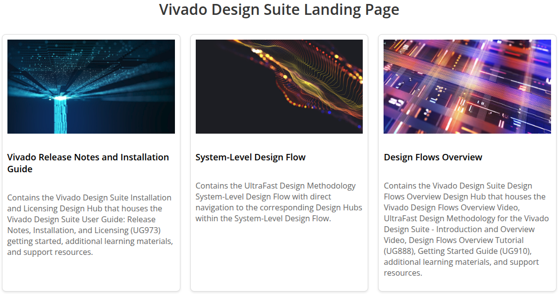
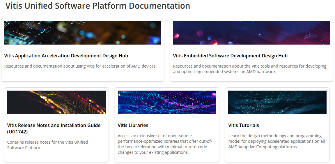
- UG1416 Vitis Unified Software Platform Documentation Landing Page. The same index for the Vitis tools.
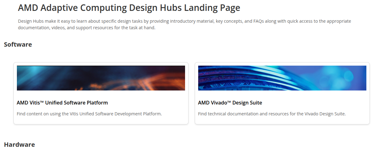
- UG1776 Adaptive Computing Design Hubs Landing Page. Design Hubs group the documents, videos, and support articles for one task, such as timing closure, IP integration, or embedded development.
- UG968 Xilinx Documentation Navigator User Guide. Documentation Navigator (DocNav) is a free desktop application for browsing, filtering, and downloading AMD documents for offline use. You can still install it with the AMD Unified Installer, but docs.amd.com is the main option when you are online.
- Adaptive Support Knowledge Base Articles on known issues, design advisories, workarounds, and release notes. These were called Answer Records on the old Xilinx site.
- Adaptive Support Community Forums Q&A forums for Vivado, Vitis, IP, embedded Linux, and devices, answered by AMD engineers and experienced users. Reading is open; posting needs a free AMD account.
-
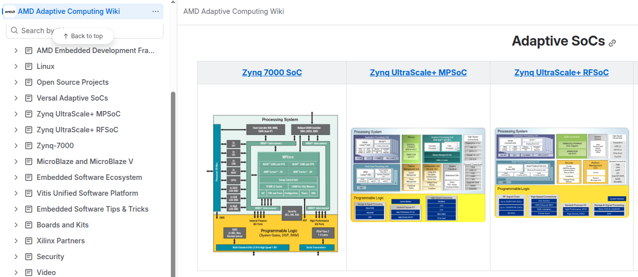
AMD Adaptive Computing Wiki AMD’s public wiki for embedded software on its adaptive SoCs: Linux and U-Boot drivers, OpenAMP, bare-metal drivers, boot flows, and board bring-up notes for Zynq 7000, Zynq UltraScale+, Versal, and Kria.
Start Here
These apply to every device family.
- UG910 Vivado Design Suite User Guide: Getting Started. A short introduction to installing, licensing, and launching Vivado, also including short videos, and links to additional resources.
- UG973 Vivado Design Suite User Guide: Release Notes, Installation, and Licensing. What is new in each release, supported operating systems and devices, system requirements, installation, and license setup.
- UG888 Vivado Design Suite Tutorial: Design Flows Overview. A hands-on tutorial that takes a small design through the full Vivado flow in both project and non-project mode.
- UG949 UltraFast Design Methodology Guide for FPGAs and SoCs. AMD’s recommended practices from board and device planning through RTL coding, clocking, resets, constraints, and timing closure. Read it before the individual Vivado user guides. For writing XDC, start with its four-step method: clocks, then input and output delays, then clock groups and CDC constraints, then timing exceptions. For timing closure, start with Baselining the Design.
- UG1292 UltraFast Design Methodology Timing Closure Quick Reference Guide. A short, printable summary of the UG949 timing closure flow: initial design checks, baselining, and resolving setup and hold violations, congestion, and clock skew.
- WP272 Get Smart About Reset: Think Local, Not Global. A 2008 white paper on why a global reset is rarely needed in FPGA designs, and how resetting only the logic that needs it saves routing and helps timing. The device examples are old, but the reasoning still applies.
Vivado Tool Flow
Most of these user guides have a companion tutorial, a separate UG that walks through the same topics on a small example design. Where one exists, it is linked at the end of the entry.
- UG892 Vivado Design Suite User Guide: Design Flows Overview. The Vivado flow from RTL to bitstream, and the difference between project mode and non-project (scripted) mode. Companion tutorial: UG888, listed in Start Here.
- UG900 Vivado Design Suite User Guide: Logic Simulation. The Vivado simulator (XSim), simulating designs that contain IP, compiling simulation libraries for third-party simulators, and running simulation in batch mode. Companion tutorial: UG937.
- UG901 Vivado Design Suite User Guide: Synthesis. Synthesis settings, supported HDL constructs, coding templates for inferring RAM, ROM, DSP blocks, and shift registers, and synthesis attributes.
- UG903 Vivado Design Suite User Guide: Using Constraints. XDC constraints: primary and generated clocks, input and output delays, timing exceptions, and physical constraints such as pin locations. It also covers the Timing Constraints Wizard, which finds missing clock, I/O, and clock domain crossing constraints. Companion tutorial: UG945.
- UG899 Vivado Design Suite User Guide: I/O and Clock Planning. Pin assignment, I/O standards and banking rules, and placement of clock resources, for existing boards and when working with a PCB designer.
- UG904 Vivado Design Suite User Guide: Implementation. The opt_design, place_design, phys_opt_design, and route_design steps, implementation strategies, and incremental implementation. Companion tutorial: UG986.
- UG906 Vivado Design Suite User Guide: Design Analysis and Closure Techniques. How to read timing, utilization, and QoR reports, analyze failing paths, and close timing. Companion tutorial: UG938.
- UG908 Vivado Design Suite User Guide: Programming and Debugging. Programming devices and configuration flash from the Hardware Manager, in-system debug with ILA, VIO, and other debug cores over JTAG, and IBERT for testing transceiver links. Companion tutorial: UG936.
- UG894 Vivado Design Suite User Guide: Using Tcl Scripting. Batch mode, querying and modifying the in-memory design, and writing reusable scripts. This is the basis for automated and CI builds.
- UG835 Vivado Design Suite Tcl Command Reference Guide. Syntax, options, and examples for every Vivado Tcl command. Use it as a lookup reference.
- UG912 Vivado Design Suite Properties Reference Guide. The properties of every Vivado object (cells, nets, pins, ports, clocks) that you query and set from Tcl and XDC. A lookup reference, like UG835.
- UG909 Vivado Design Suite User Guide: Dynamic Function eXchange. Reconfiguring part of the device while the rest keeps running, formerly called partial reconfiguration. An advanced topic; read it when a project needs it.
Power Estimation and Analysis
Estimate power early to size the power supplies and cooling, then check it against the real design in Vivado.
- UG1556 Power Design Manager User Guide. Power Design Manager (PDM) is AMD’s power and thermal estimator for UltraScale+ and Versal devices, covering the programmable logic, processing system, transceivers, memory interfaces, and AI Engines.
- UG440 Xilinx Power Estimator User Guide. XPE is the spreadsheet-based estimator for use before a design exists. AMD now points to PDM for UltraScale+ and Versal, so use XPE for 7 series, Zynq 7000, and UltraScale devices.
- UG907 Vivado Design Suite User Guide: Power Analysis and Optimization. Power analysis on the synthesized or implemented design, vectorless or driven by simulation activity (SAIF), and the power optimization options in Vivado.
IP and Interfaces
Using and Creating IP
- UG896 Vivado Design Suite User Guide: Designing with IP. The IP catalog, customizing IP, generating output products, out-of-context synthesis, simulating IP, and upgrading IP between Vivado releases. Companion tutorial: UG939.
- UG1118 Vivado Design Suite User Guide: Creating and Packaging Custom IP. How to package your own RTL as reusable IP with the IP Packager, including bus interfaces, parameters, and custom IP repositories. Companion tutorial: UG1119.
- UG994 Vivado Design Suite User Guide: Designing IP Subsystems Using IP Integrator. Building block designs: connection automation, address maps, parameter propagation, and the generated HDL wrapper. This is where a Zynq processing system gets connected to your logic. Companion tutorial: UG995.
AXI
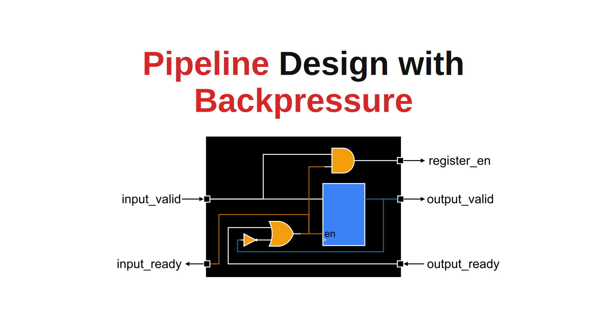
Most AMD IP uses the Arm AMBA AXI interfaces. Before writing custom AXI logic, read the handshake rules in the Arm specification and simulate your design against the AXI Verification IP. The ready/valid handshake itself is explained in our post on pipeline design with backpressure.
- UG1037 Vivado Design Suite: AXI Reference Guide. An introduction to AXI4, AXI4-Lite, and AXI4-Stream as used in AMD IP and tools, including handshake rules and infrastructure IP. Last revised in 2017.
- IHI 0022 H.c AMBA AXI and ACE Protocol Specification (Arm). The normative definition of AXI3, AXI4, and AXI4-Lite. Issue H.c is the last issue that includes AXI4 and AXI4-Lite; later issues describe only the AXI5 family, so use this one for AMD IP.
- IHI 0051 AMBA AXI-Stream Protocol Specification (Arm). Defines AXI4-Stream and AXI5-Stream: the TVALID/TREADY handshake and the TLAST, TKEEP, and TUSER side-band signals used by most streaming, video, and HLS IP.
- PG267 AXI Verification IP LogiCORE IP Product Guide. A SystemVerilog model that acts as an AXI master, slave, or pass-through monitor for simulating custom AXI IP and block designs.
IP Product Guides
Every IP core in the Vivado IP catalog has a product guide. These are the ones most designs use.
Clocking and On-Chip Memory
- PG065 Clocking Wizard LogiCORE IP Product Guide. Configures the MMCM and PLL primitives to generate clocks with the required frequency, phase, and jitter.
- PG057 FIFO Generator v13.2 Product Guide. Synchronous and asynchronous (clock-crossing) FIFOs with native or AXI interfaces, built from block RAM, distributed RAM, or built-in FIFO primitives.
- PG058 Block Memory Generator v8.4 Product Guide. Single-port and dual-port RAM and ROM built from block RAM, including memory initialization with COE files.
Debug
- PG172 Integrated Logic Analyzer v6.2 Product Guide. Probe configuration, trigger and storage qualification options, and capture depth for the ILA. Read it alongside UG908.
- PG159 Virtual Input/Output v3.0 Product Guide. The VIO core reads and drives internal signals from the Hardware Manager over JTAG, which helps on boards with few buttons and LEDs.
AXI Infrastructure and DMA
- PG059 AXI Interconnect LogiCORE IP Product Guide. Connects AXI memory-mapped masters and slaves, with width, clock, and protocol converters, register slices, and data FIFOs.
- PG247 SmartConnect LogiCORE IP Product Guide. The interconnect that IP Integrator uses by default in newer designs. It inserts width, clock, and protocol conversion automatically.
- PG085 AXI4-Stream Infrastructure IP Suite LogiCORE IP Product Guide. The AXI4-Stream helper cores: data FIFO, clock converter, data width converter, register slice, broadcaster, combiner, and switch.
- PG021 AXI DMA LogiCORE IP Product Guide. Moves data between memory and AXI4-Stream logic in simple or scatter-gather mode. It is the usual way to connect streaming logic in the PL to the Zynq processing system.
Processors
- PG082 Processing System 7 v5.5 Product Guide. The Zynq 7000 processing system IP in IP Integrator: PS-PL AXI ports, clocks, resets, interrupts, MIO and EMIO pin routing, and DDR settings.
- PG201 Zynq UltraScale+ MPSoC Processing System Product Guide. The same for Zynq UltraScale+: PS-PL AXI interfaces, clocks, resets, interrupts, MIO configuration, and DDR settings.
- UG1629 MicroBlaze V Processor Reference Guide. AMD’s RISC-V based soft processor and the successor to classic MicroBlaze for new designs.
- UG984 MicroBlaze Processor Reference Guide. The classic MicroBlaze soft processor, still found in many existing designs. AMD EDF does not support it for Linux.
Memory Controllers
- UG586 Zynq 7000 SoC and 7 Series Devices Memory Interface Solutions User Guide. The MIG IP for DDR3, DDR2, LPDDR2, QDR II+, and RLDRAM II/3 on 7 series devices: controller configuration, simulation, pinout rules, and PCB guidelines. It is a UG, not a PG, even though it documents an IP core.
- PG150 UltraScale Architecture-Based FPGAs Memory IP LogiCORE IP Product Guide. The memory interface IP for UltraScale and UltraScale+ FPGAs (DDR3, DDR4, LPDDR3, QDR II+, QDR-IV, and RLDRAM 3), including configuration, pin and bank rules, and simulation.
PCI Express
- PG054 7 Series FPGAs Integrated Block for PCI Express LogiCORE IP Product Guide. The Gen1/Gen2 PCIe hard block in 7 series FPGAs, for endpoint and root port designs.
- PG156 UltraScale Devices Gen3 Integrated Block for PCI Express LogiCORE IP Product Guide. The Gen3 PCIe hard block in UltraScale devices.
- PG213 UltraScale+ Devices Integrated Block for PCI Express v1.3 Product Guide. The PCIe hard block in UltraScale+ devices, used directly for endpoint or root port designs and underneath the DMA subsystems.
- PG195 DMA/Bridge Subsystem for PCI Express Product Guide. The XDMA IP: a scatter-gather DMA engine and AXI bridge between a PCIe host and AXI memory-mapped or AXI4-Stream logic in the FPGA.
Ethernet
- PG138 AXI 1G/2.5G Ethernet Subsystem Product Guide. A tri-mode 10/100/1000 Mb/s MAC with 2.5G support, MII, GMII, RGMII, SGMII, or 1000BASE-X PHY interfaces, AXI4-Stream data paths, and AXI4-Lite control.
- PG210 10G/25G High Speed Ethernet Subsystem Product Guide. The 10G/25G Ethernet MAC and PCS for UltraScale and UltraScale+ devices.
- PG203 UltraScale+ Devices Integrated 100G Ethernet Subsystem LogiCORE IP Product Guide. The wrapper for the 100G Ethernet hard block (CMAC), with optional RS-FEC and an AXI4-Stream user interface. UltraScale devices use PG165.
Device Architecture
Read the set for the family you use. Pick the device with the overview data sheet, check pins and electrical limits in the packaging guide and the DC and AC switching data sheet, and read the core fabric guides (CLB, clocking, memory, I/O) before writing RTL for that family.
7 Series
This covers Spartan 7, Artix 7, Kintex-7, and Virtex-7. The fabric guides also apply to the programmable logic in Zynq 7000 devices; the Zynq-specific documents are in the SoCs section.
Choose a device
- DS180 7 Series FPGAs Data Sheet: Overview. Resources per device, device-package combinations with maximum I/O, and which packages are footprint compatible, so you can move to a larger device later without changing the board.
- UG475 7 Series FPGAs Packaging and Pinout Product Specification. Pin definitions, ASCII pinout files, and bank diagrams for every device and package.
- DC and AC switching characteristics (operating conditions, power supplies, I/O, and timing by speed grade), one data sheet per family:
Core fabric guides
- UG474 7 Series FPGAs Configurable Logic Block User Guide. SLICEL and SLICEM structure, 6-input LUTs, flip-flops, carry chains, wide multiplexers, distributed RAM, and shift registers.
- UG472 7 Series FPGAs Clocking Resources User Guide. Global, regional, and I/O clock networks, the clock buffers (BUFG, BUFH, BUFR, BUFIO), and the MMCM and PLL blocks.
- UG473 7 Series FPGAs Memory Resources User Guide. Block RAM (36 Kb blocks usable as two 18 Kb blocks, true and simple dual-port modes, cascading, ECC) and the FIFO logic built into the block RAM.
- UG471 7 Series FPGAs SelectIO Resources User Guide. I/O banks, single-ended and differential I/O standards, DCI, and the I/O logic (IDELAY, ODELAY, ISERDES, OSERDES). Read it before pin planning or building source-synchronous interfaces.
Read when needed
- UG479 7 Series DSP48E1 Slice User Guide. The 25 x 18 multiplier, pre-adder, 48-bit ALU and accumulator, pattern detector, and cascade paths, with guidance for filters and other arithmetic.
- UG476 7 Series FPGAs GTX/GTH Transceivers User Guide. The GTX and GTH transceivers in Kintex-7, Virtex-7, and Zynq Z-7030 and larger devices.
- UG482 7 Series FPGAs GTP Transceivers User Guide. The GTP transceivers in Artix 7 FPGAs and the Zynq Z-7012S and Z-7015. Spartan 7 has no transceivers.
- UG480 7 Series FPGAs and Zynq-7000 SoC XADC Dual 12-Bit 1 MSPS Analog-to-Digital Converter User Guide. The XADC block: two 12-bit ADCs, on-chip temperature and supply sensors, and alarms.
- UG470 7 Series FPGAs Configuration User Guide. Configuration modes (SPI, BPI, SelectMAP, serial, JTAG), bitstream encryption, MultiBoot and fallback, and readback. Needed when you design a board or write flash-programming software.
- UG483 7 Series FPGAs PCB Design Guide. Power distribution and decoupling, PCB materials and traces, and signal integrity. Zynq 7000 boards use UG933.
- UG953 Vivado Design Suite 7 Series FPGA and Zynq 7000 SoC Libraries Guide. Every design primitive (IBUFDS, IDELAYE2, MMCME2_ADV, RAMB36E1, and more) and the XPM macros (XPM_CDC, XPM_FIFO, XPM_MEMORY), with Verilog and VHDL instantiation templates.
UltraScale and UltraScale+
This covers Kintex and Virtex UltraScale and the UltraScale+ families (Spartan, Artix, Kintex, and Virtex). Most guides are shared across all of them. Spartan UltraScale+ has its own configuration and SelectIO guides, listed at the end.
Choose a device
- DS890 UltraScale Architecture and Product Data Sheet: Overview. Resource tables, device-package combinations, and migration notes for every UltraScale and UltraScale+ family.
- UG575 UltraScale+ Device Packaging and Pinouts Product Specification User Guide. Package drawings, pin definitions, and pinout files for the FPGA families. Zynq UltraScale+ devices use UG1075.
- DC and AC switching characteristics, one data sheet per family:
- DS892 Kintex UltraScale FPGAs Data Sheet: DC and AC Switching Characteristics.
- DS893 Virtex UltraScale FPGAs Data Sheet: DC and AC Switching Characteristics.
- DS930 Spartan UltraScale+ FPGA Data Sheet: DC and AC Switching Characteristics.
- DS931 Artix UltraScale+ FPGA Data Sheet: DC and AC Switching Characteristics.
- DS922 Kintex UltraScale+ FPGAs Data Sheet: DC and AC Switching Characteristics.
- DS923 Virtex UltraScale+ FPGA Data Sheet: DC and AC Switching Characteristics.
Core fabric guides
- UG574 UltraScale Architecture Configurable Logic Block User Guide. 6-input LUTs, flip-flops, carry chains, wide multiplexers, distributed RAM, and shift registers.
- UG572 UltraScale Architecture Clocking Resources User Guide. Clock routing and distribution, the clock buffers (BUFGCE, BUFGCTRL, BUFG_GT), and the MMCM and PLL blocks.
- UG573 UltraScale Architecture Memory Resources User Guide. Block RAM, built-in FIFO, and UltraRAM: configurations, cascading, and ECC.
- UG571 UltraScale Architecture SelectIO Resources User Guide. The HP, HR, and HD I/O banks, I/O standards, and I/O logic (delays, SERDES, and native-mode byte groups).
Read when needed
- UG579 UltraScale Architecture DSP Slice User Guide. The DSP48E2 slice: 27 x 18 multiplier, pre-adder, 48-bit ALU, wide XOR, and cascade paths.
- UG576 UltraScale Architecture GTH Transceivers User Guide. GTH transceivers up to 16.3 Gb/s: PLLs, TX and RX datapaths, equalization, and clocking.
- UG578 UltraScale Architecture GTY Transceivers User Guide. GTY transceivers, up to 32.75 Gb/s in UltraScale+.
- UG581 Virtex UltraScale+ FPGAs GTM Transceivers User Guide. PAM4 and NRZ transceivers up to 58 Gb/s, found only in the VU23P, VU27P, VU29P, and VU57P.
- UG580 UltraScale Architecture System Monitor User Guide. The SYSMON block: ADC, on-chip temperature and supply sensors, and alarms.
- UG570 UltraScale Architecture Configuration User Guide. Configuration modes, bitstream security, MultiBoot, and readback. Zynq UltraScale+ boot is covered in UG1085, and Spartan UltraScale+ uses UG860.
- UG583 UltraScale Architecture PCB Design User Guide. Power distribution, decoupling, and layout guidelines for memory interfaces and transceivers, plus device migration details.
- UG974 UltraScale Architecture Libraries Guide. Every UltraScale and UltraScale+ design primitive and the XPM macros, with Verilog and VHDL instantiation templates.
Spartan UltraScale+ only
- UG860 Spartan UltraScale+ FPGAs Configuration User Guide. Configuration modes, boot methods, and configuration security.
- UG861 Spartan UltraScale+ FPGAs SelectIO Resources User Guide. I/O bank types, I/O standards, and I/O logic.
Versal
Versal devices document their hardware blocks in architecture manuals (AM) instead of user guides.
Choose a device
- DS950 Versal Architecture and Product Data Sheet: Overview. Resources per device, device-package combinations, and a summary of each architectural block, for every Versal series including Gen 2.
- AM013 Versal Adaptive SoC Packaging and Pinouts Architecture Manual. Package drawings, pin definitions, and pinout files.
- DC and AC switching characteristics, one data sheet per series:
- DS956 Versal Prime Series Data Sheet: DC and AC Switching Characteristics.
- DS957 Versal AI Core Series Data Sheet: DC and AC Switching Characteristics.
- DS958 Versal AI Edge Series Data Sheet: DC and AC Switching Characteristics.
- DS959 Versal Premium Series Data Sheet: DC and AC Switching Characteristics.
- DS960 Versal HBM Series Data Sheet: DC and AC Switching Characteristics.
- DS1020 Versal Prime Series Gen 2 Data Sheet: DC and AC Switching Characteristics.
- DS1021 Versal AI Edge Series Gen 2 Data Sheet: DC and AC Switching Characteristics.
Core fabric guides
- AM005 Versal Adaptive SoC Configurable Logic Block Architecture Manual. LUTs, flip-flops, carry logic, distributed RAM, and shift registers.
- AM003 Versal Adaptive SoC Clocking Resources Architecture Manual. Clock buffers and routing, and the MMCM, DPLL, and XPLL blocks.
- AM007 Versal Adaptive SoC Memory Resources Architecture Manual. Block RAM and UltraRAM: configurations, cascading, and ECC.
- AM010 Versal Adaptive SoC SelectIO Resources Architecture Manual. The XPIO and HDIO banks, supported I/O standards, and the I/O logic.
Read when needed
- AM004 Versal ACAP DSP Engine Architecture Manual. The DSP58 engine: 27 x 24 multiplier, 58-bit accumulator, and the floating-point and complex arithmetic modes.
- AM002 Versal Adaptive SoC GTY and GTYP Transceivers Architecture Manual. The GTY and GTYP serial transceivers.
- AM017 Versal Adaptive SoC GTM Transceivers Architecture Manual. The PAM4 GTM transceivers, in the devices that have them.
- AM006 Versal Adaptive SoC System Monitor Architecture Manual. On-chip temperature and supply sensors and up to 17 external analog inputs.
Methodology
Versal replaces UG949 with a set of methodology guides, one for each stage of a project.
- UG1504 Versal Adaptive SoC System and Solution Planning Methodology Guide. Planning a system around the application before implementation: device selection and partitioning across the PL, PS, AI Engines, and NoC.
- UG1387 Versal Adaptive SoC Hardware, IP, and Platform Development Methodology Guide. Recommended practices for design entry, so the design uses the device resources efficiently.
- UG1388 Versal Adaptive SoC System Integration and Validation Methodology Guide. Timing closure, power closure, and system validation.
- UG1506 Versal Adaptive SoC Board System Design Methodology Guide. PCB, power delivery, and other board-level considerations.
SoCs
If your device has a hard processor, add the documents for its family. Each family has an overview data sheet, a hardware reference (the Technical Reference Manual, or TRM), a register reference, a software guide, and an embedded design tutorial.
Zynq 7000 SoC
- DS190 Zynq-7000 SoC Data Sheet: Overview. The single- or dual-core Cortex-A9 processing system, programmable logic resources per device, and device-package combinations.
- DS187 Zynq-7000 SoC (Z-7007S, Z-7012S, Z-7014S, Z-7010, Z-7015, and Z-7020): DC and AC Switching Characteristics Data Sheet. Electrical and timing specifications for the PS and PL of the smaller devices, including the Z-7010 and Z-7020 found on most teaching boards.
- DS191 Zynq-7000 SoC (Z-7030, Z-7035, Z-7045, and Z-7100): DC and AC Switching Characteristics Data Sheet. The same for the larger devices.
- UG585 Zynq 7000 SoC Technical Reference Manual. Hardware reference for the processing system: boot and PL configuration, memory map, interconnect, peripherals, clocks, resets, and PS-PL interfaces, with register descriptions for every PS module.
- UG821 Zynq 7000 SoC Software Developers Guide. The software view: boot flow and FSBL, board support packages, operating system options, and the development tools.
- UG1165 Zynq 7000 Embedded Design Tutorial. A step-by-step embedded design in Vivado and Vitis, from hardware platform to running software.
- UG865 Zynq-7000 SoC Packaging and Pinout Product Specification. Pin definitions, pinout files, and package drawings.
- UG933 Zynq-7000 SoC PCB Design Guide. Power distribution, decoupling, and layout for the PS and PL interfaces.
Zynq UltraScale+ MPSoC and RFSoC
- DS891 Zynq UltraScale+ MPSoC Data Sheet: Overview. Processing system options (dual- or quad-core Cortex-A53, dual Cortex-R5F, and a GPU and video codec on some devices) and PL resources per device.
- DS925 Zynq UltraScale+ MPSoC Data Sheet: DC and AC Switching Characteristics. Electrical and timing specifications for the PS and PL.
- UG1085 Zynq UltraScale+ Device Technical Reference Manual. Hardware reference for the processing system: Cortex-A53 APU, Cortex-R5F RPU, GPU where present, PMU, CSU, boot, memory map, and peripherals, for MPSoC and RFSoC devices.
- UG1087 Zynq UltraScale+ Devices Register Reference. Addresses, bit fields, and reset values for every PS register.
- UG1137 Zynq UltraScale+ MPSoC Software Developer Guide. Boot flow and FSBL, PMU firmware, Arm Trusted Firmware, bare-metal and Linux software stacks, SMP and AMP (OpenAMP), hypervisors, and security features.
- UG1209 Zynq UltraScale+ MPSoC Embedded Design Tutorial. A step-by-step embedded design on the ZCU102 board using Vivado and Vitis.
- UG1075 Zynq UltraScale+ Device Packaging and Pinouts Product Specification User Guide. Packaging and pinouts for MPSoC and RFSoC devices.
- For RFSoC devices, which add RF data converters, use these data sheets instead of DS891 and DS925:
Versal Adaptive SoC
The overview and DC and AC data sheets are listed under Versal in the device section.
- UG1273 Versal Adaptive SoC Design Guide. An overview of the Versal hardware features and block-level considerations for new or migrated designs, with recommendations on design flows, simulation, debug, and boot.
- AM011 Versal Adaptive SoC Technical Reference Manual. Hardware reference for first-generation Versal devices: PMC and boot, the processing system (Cortex-A72 APU and Cortex-R5F RPU), interconnect including the NoC, memory controllers, peripherals, clocks, and resets.
- AM012 Versal Adaptive SoC Register Reference. Register-level reference for the PS, PMC, and related hard blocks.
- PG313 Versal Adaptive SoC Programmable Network on Chip and Integrated Memory Controller 1.1 LogiCORE IP Product Guide. Configuring the NoC and the hard DDR memory controllers through the AXI NoC IP: connectivity, QoS, and memory controller settings.
- UG1304 Versal Adaptive SoC System Software Developers Guide. Boot flow, platform management firmware, software stacks, and system software components.
- UG1305 Versal Adaptive SoC Embedded Design Tutorial. A hands-on embedded design for the VCK190, VMK180, and VPK180 evaluation boards using Vivado and Vitis.
- Versal AI Edge Series Gen 2 and Prime Series Gen 2 devices use these instead of AM011, AM012, and PG313:
- AI Engines come in three generations: AIE, AIE-ML, and AIE-ML v2. DS950 tells you which one your device has. Read the architecture manual for that engine, then the tools guide and the matching programming guide:
- AM009 Versal Adaptive SoC AI Engine Architecture Manual.
- AM020 Versal Adaptive SoC AIE-ML Architecture Manual.
- AM027 Versal Adaptive SoC AIE-ML v2 Architecture Manual.
- UG1076 AI Engine Tools and Flows User Guide.
- UG1079 AI Engine Kernel and Graph Programming Guide.
- UG1603 AI Engine-ML Kernel and Graph Programming Guide.
Embedded Software
- UG1400 Vitis Unified Software Platform Documentation: Embedded Software Development. Embedded software in the Vitis Unified IDE: creating a platform from a Vivado XSA, configuring the BSP, building and debugging bare-metal and Linux applications, and creating boot images.
- UG1283 Bootgen User Guide. Bootgen and the BIF file format used to build boot images (BOOT.BIN) for Zynq 7000, Zynq UltraScale+, and Versal, including encryption and authentication.
- UG1606 OS and Libraries Help: BSP and Libraries Document Collection. API documentation for the standalone BSP, the peripheral drivers (GPIO, AXI DMA, UART, and others), and libraries such as lwIP and xilffs used in bare-metal applications.
- UG1144 PetaLinux Tools Documentation: Reference Guide. PetaLinux, AMD’s Yocto-based tool for building embedded Linux images. AMD has scheduled PetaLinux for deprecation in the 2026.2 release and recommends AMD EDF for new projects.
- AMD EDF AMD Embedded Development Framework Documentation. The Yocto Project based framework that replaces PetaLinux, with development flows, walkthroughs, and a PetaLinux to EDF migration guide.
HLS and Libraries
- UG1399 Vitis High-Level Synthesis User Guide. How to write C/C++ for HLS and optimize it with pipelining, loop unrolling, array partitioning, dataflow, and interface synthesis. For small working examples, see the Vitis HLS Introductory Examples in Part 1.
- UG1702 Vitis Reference Guide. Its HLS Pragmas chapter gives the complete syntax of every HLS pragma; UG1399 explains when to use them.
- Vitis Libraries Open-source C++ libraries for Vitis, provided as HLS primitives (L1), kernels (L2), and host APIs (L3). The source is on GitHub. The most useful ones for HLS are:
Background Papers
- Clifford Cummings’ papers Classic SNUG papers on clock domain crossing, asynchronous FIFO design, resets, and RTL coding style. They complement WP272 and are useful on any FPGA or ASIC. The papers are hosted in the Paradigm Works Technical Library; downloads need a free account.
Suggested Reading Order
- UG910 and UG973 to install the tools, then UG888 to take one small design through the full flow.
- UG949 (the RTL coding, clocking, and reset chapters) and WP272.
- The CLB, clocking, and memory guides for your family, for example UG474, UG472, and UG473 for 7 series.
- UG903, its tutorial UG945, and the UG949 four-step method as soon as you write your first constraints; UG906 and UG1292 when timing fails.
- Before your first block design: UG994, UG1037, and the Arm AXI specification. On a Zynq board, add your family’s TRM and UG1400.
- Everything else as you need it.
I checked every link in this post on October 2026. AMD moves documents from time to time; if a link breaks, search docs.amd.com for the document number. For more tutorials, see AICLAB Resources.